Printed Circuit Board Assembly Plants: Explore the Electronics Manufacturing Process
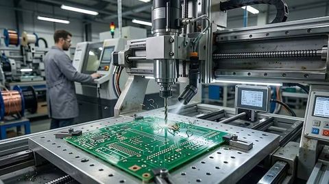
Printed circuit board assembly plants play a central role in turning electronic designs into functional products.
From industrial control equipment and communication devices to medical instruments and consumer electronics, these facilities assemble electronic components onto circuit boards that enable devices to perform their intended functions.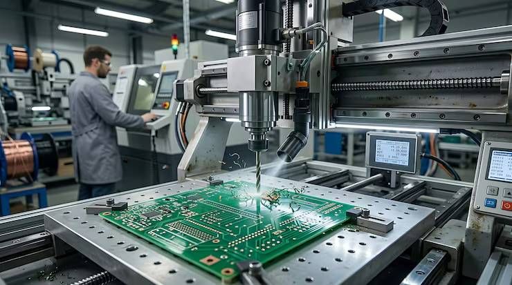
As electronic products become more compact and complex, assembly plants must coordinate precision machinery, component handling, soldering processes, inspection systems, and production planning. Even a small placement error or soldering defect can affect the reliability of the finished electronic assembly.
Understanding how printed circuit board assembly works helps explain the relationship between circuit design, manufacturing technology, quality control, and final product performance. The process moves through several connected stages, beginning with bare circuit boards and electronic components and ending with tested assemblies ready for integration into larger products.
How Printed Circuit Board Assembly Begins
A printed circuit board (PCB) provides the physical platform and electrical connections needed to connect electronic components. The bare board contains conductive copper pathways separated by insulating materials, allowing electrical signals and power to travel between designated points.
PCB assembly, commonly called PCBA, begins when electronic components are mounted onto this prepared board. Components may include resistors, capacitors, integrated circuits, connectors, processors, and power-management devices. Their placement must follow the circuit design and the manufacturer's assembly documentation.
Before production starts, engineers review the bill of materials, board layout, component specifications, assembly drawings, and manufacturing requirements. The bill of materials identifies the components required for the assembly, while the layout establishes where each component belongs.
This preparation helps identify potential issues before they interrupt production. Component availability, package dimensions, soldering requirements, board complexity, and inspection needs can all influence how the assembly line is configured.
Preparing the Board and Electronic Components
Material preparation establishes the conditions needed for accurate assembly. Bare PCBs must be handled carefully to prevent contamination, physical damage, and problems that could affect soldering or electrical performance.
Electronic components also require appropriate storage and handling. Some surface-mount devices are moisture-sensitive, meaning they can absorb moisture from the surrounding environment. If these components are exposed to excessive moisture and then heated rapidly during soldering, internal damage can occur.
Manufacturers follow component-specific handling instructions, including moisture-control procedures where required. This may involve dry storage, controlled exposure times, and baking under specified conditions when necessary.
Production teams also verify component identification and orientation. Incorrect part numbers, mixed component values, or improperly oriented polarized components can lead to functional failures. Barcode systems and digital production records can help confirm that the correct materials reach the assembly line.
Surface-Mount Technology and Automated Placement
Surface-mount technology (SMT) is widely used in modern PCB assembly because it supports compact components and high-speed automated production. In this process, components are mounted directly onto designated pads on the board rather than relying primarily on leads inserted through drilled holes.
The SMT process usually begins with solder paste printing. A stencil aligns with the PCB, allowing controlled amounts of solder paste to be deposited onto the appropriate pads. The paste contains tiny solder particles suspended in a flux mixture that supports the soldering process.
A solder paste inspection system may then check whether the deposits have the correct volume, position, and shape. Detecting printing problems at this stage can prevent defects from continuing through the production line.
Next, automated pick-and-place machines position components onto the solder paste. These machines use programmed coordinates, component feeders, cameras, and alignment systems to place parts accurately, including very small components with closely spaced connections.
The assembled board then moves to the reflow soldering stage, where a controlled temperature profile melts the solder paste and forms electrical and mechanical connections between components and the board.
Reflow Soldering and Thermal Control
Reflow soldering requires more than simply heating a board until the solder melts. The temperature profile must suit the solder paste, PCB construction, and components being assembled.
A typical reflow process includes controlled heating, thermal soaking where appropriate, a peak-temperature stage, and cooling. Each phase influences how the solder behaves and how the components experience thermal stress.
Insufficient heating can produce incomplete solder joints, while excessive temperatures may damage sensitive components or the board itself. Uneven heating can also create defects, particularly when a board contains components of different sizes and thermal characteristics.
Manufacturers develop and verify suitable profiles for their assemblies. Temperature sensors and thermal profiling equipment can help confirm that different locations on the board receive appropriate heating during production.
Once soldering is complete, the board can proceed to inspection. Some assemblies require additional cleaning, depending on the soldering materials, flux chemistry, and cleanliness requirements.
Through-Hole Assembly and Mixed Technology Boards
Not every electronic component is mounted using surface-mount technology. Through-hole assembly remains important for components that require particular mechanical strength, connector arrangements, or electrical characteristics.
In through-hole assembly, component leads pass through holes in the PCB and are soldered to conductive pads. Depending on the design and production requirements, components may be inserted manually or by automated equipment.
Wave soldering is one established method for soldering suitable through-hole assemblies. The board passes over a controlled wave of molten solder, which forms connections between component leads and the board's conductive surfaces.
Selective soldering is used when only specific areas require soldering, particularly on mixed-technology boards where surface-mount components are already installed. The process directs solder to designated locations while reducing unnecessary thermal exposure to nearby components.
Many products combine SMT and through-hole technologies. The manufacturing sequence must account for component placement, soldering order, thermal limits, and access to the areas that require inspection.
Inspecting and Testing Assembled Circuit Boards
Quality control is integrated throughout PCB assembly rather than being limited to the final stage. Different inspection methods identify different categories of defects, so manufacturers often combine several techniques.
Automated optical inspection (AOI) uses cameras and image-processing software to examine component placement, orientation, solder joints, and visible assembly features. It can identify issues such as missing components, misalignment, and certain soldering defects.
X-ray inspection can reveal hidden solder connections that are difficult or impossible to examine optically. This is particularly useful for packages such as ball grid arrays, where solder joints sit beneath the component body.
Electrical testing adds another layer of verification. In-circuit testing can check selected electrical connections and component characteristics, while functional testing evaluates whether the assembled board behaves as intended under defined operating conditions.
These methods serve different purposes. A board may appear visually correct but still contain an electrical fault, while a successful electrical test does not necessarily identify every potential long-term reliability issue. Inspection and testing plans should therefore reflect the product's design, complexity, and application.
Production Planning and Traceability
Assembly plants must coordinate machinery, materials, operators, and inspection capacity to maintain a consistent production flow. Poor coordination can lead to machine downtime, material shortages, excessive work in progress, or delays between manufacturing stages.
Production planning considers factors such as board complexity, machine setup, component feeder configuration, soldering capacity, and testing requirements. Product changeovers also need careful management because different PCB designs may require different programs, stencils, components, and process settings.
Traceability helps manufacturers investigate defects and manage product quality. Depending on the production system, records may connect an individual board or batch with component lots, machine programs, soldering profiles, inspection results, and test outcomes.
This information becomes especially valuable when a defect appears after products have entered service. Engineers can use manufacturing records to identify potentially affected assemblies, investigate the cause, and determine whether corrective action is necessary.
How Assembly Plants Support Product Reliability
PCB assembly quality depends on the interaction between design, materials, machinery, and process control. A well-configured production line cannot fully compensate for unsuitable component selection or a board layout that creates difficult manufacturing conditions.
Design for manufacturability helps engineers consider assembly requirements during the product development stage. Adequate component spacing, accessible inspection points, appropriate pad geometry, and realistic thermal requirements can make production more consistent.
Manufacturers may also use process-control methods and industry standards to establish repeatable procedures. IPC standards, for example, provide widely used frameworks for electronic assembly workmanship, acceptance criteria, and related manufacturing practices. The applicable requirements depend on the product and the agreement between the manufacturer and customer.
Continuous improvement draws on inspection data, production records, and failure analysis. When recurring defects are identified, teams can investigate whether the underlying cause involves stencil design, component handling, soldering parameters, equipment calibration, or board layout.
Frequently Asked Questions
What is a PCB assembly plant?
A PCB assembly plant is a manufacturing facility where electronic components are mounted and connected to printed circuit boards using processes such as solder paste printing, component placement, soldering, inspection, and electrical testing.
What is the difference between PCB and PCBA?
A PCB is the bare circuit board with conductive pathways and connection points. A PCBA is the assembled board after electronic components have been mounted and soldered into place.
Why is SMT widely used in electronics manufacturing?
Surface-mount technology supports compact component designs, automated placement, and efficient high-volume production. It is suitable for many modern electronic products that require dense component layouts.
How do manufacturers check PCB assembly quality?
Manufacturers use methods such as automated optical inspection, X-ray inspection, in-circuit testing, and functional testing. The combination depends on the board design, component packages, and reliability requirements.
Can one assembly plant produce different types of circuit boards?
Yes. Many plants handle multiple board designs and product categories by adjusting equipment programs, component feeders, stencils, soldering profiles, and testing procedures. The range of products depends on the facility's equipment and process capabilities.
Conclusion
Printed circuit board assembly plants combine precision machinery, electronic components, controlled soldering, and systematic testing to produce functional electronic assemblies. Each stage contributes to the accuracy, electrical performance, and reliability of the finished board.
As electronic products become more sophisticated, successful assembly increasingly depends on coordinated engineering, automation, traceability, and quality control. Understanding these processes provides a clearer picture of how modern electronics move from circuit-board designs to dependable working products.

Related Post...
Medical Imaging Equipment Vendors Explore Solutions for Better Diagnostic Workflows
Updated: October 19, 2026
Read More
Automated CNC Milling Machine Suppliers: Insights Into Equipment Selection
Updated: October 02, 2026
Read More
Die Casting Manufacturing Equipment: Explore Machines and Production Processes
Updated: October 02, 2026
Read More