Microchip Manufacturing: Process, Technology, Equipment, and Applications
Microchip manufacturing is one of the most advanced processes in modern electronics production.
Microchips, also known as integrated circuits or semiconductor chips, are essential components in computers, smartphones, automobiles, medical equipment, industrial machinery, and communication devices.
These tiny electronic components contain millions or billions of transistors and other circuit elements that process information, store data, and control electronic systems.
The manufacturing process involves advanced engineering, specialized materials, precision machinery, and highly controlled production environments. Semiconductor manufacturers use sophisticated technologies to create extremely small electronic structures on silicon wafers.
As demand for artificial intelligence, cloud computing, electric vehicles, automation, and connected devices continues to grow, microchip manufacturing has become increasingly important to the global technology industry.
What Is Microchip Manufacturing?
Microchip manufacturing is the process of designing, fabricating, assembling, and testing semiconductor devices used in electronic systems.
The process begins with semiconductor materials, commonly silicon, which are processed to create complex electronic circuits.
Manufacturers build microscopic structures on semiconductor wafers using techniques such as photolithography, deposition, etching, doping, and polishing.
Once the electronic circuits are formed, the wafers are tested and separated into individual chips. These chips are then packaged and tested again before being supplied to electronics manufacturers.
Microchip manufacturing requires precise control over temperature, pressure, chemical processes, particle contamination, and manufacturing conditions.
Main Materials Used in Microchip Manufacturing
Semiconductor production depends on specialized materials that support the formation of electronic circuits.
1. Silicon Wafers
Silicon is the most widely used semiconductor material in conventional microchip manufacturing.
It is processed into thin, circular wafers that provide the foundation for building integrated circuits.
Wafer quality, surface flatness, crystal structure, and cleanliness directly influence manufacturing performance.
2. Photoresist Materials
Photoresist is a light-sensitive chemical coating used during photolithography.
It helps transfer circuit patterns onto the wafer surface through controlled exposure and development processes.
3. Conductive Materials
Materials such as copper, aluminum, and other specialized metals are used to create electrical connections within semiconductor devices.
4. Insulating Materials
Insulating materials separate conductive structures and help prevent unwanted electrical interactions.
Examples include silicon dioxide and other advanced dielectric materials.
5. Doping Materials
Dopants are introduced into selected regions of semiconductor materials to modify their electrical properties.
Common dopants include boron, phosphorus, and arsenic.
6. Process Chemicals and Gases
Semiconductor fabrication uses highly purified chemicals and specialty gases for cleaning, etching, deposition, and other manufacturing operations.
Strict material handling and contamination controls are essential throughout production.
How Does Microchip Manufacturing Work?
Microchip manufacturing involves several interconnected stages, from circuit design to final product testing.
Major stages of semiconductor production
1. Chip Design
The manufacturing process begins with electronic circuit design.
Engineers define the chip's functionality, architecture, performance requirements, power consumption, and physical layout.
Specialized electronic design automation (EDA) software helps engineers develop and verify complex circuit designs before fabrication.
The completed design is converted into manufacturing information used to create the chip.
2. Silicon Wafer Preparation
High-purity silicon is processed into single-crystal ingots.
These ingots are sliced into thin wafers, which are polished to create smooth surfaces suitable for semiconductor fabrication.
Before processing, wafers undergo cleaning and inspection to identify surface defects or contamination.
3. Photolithography
Photolithography is one of the most important processes in microchip manufacturing.
A photoresist coating is applied to the wafer and exposed to a patterned light source through a photomask or reticle.
The exposed or unexposed regions are developed according to the resist chemistry.
This process transfers extremely detailed circuit patterns onto the wafer.
Advanced semiconductor facilities use sophisticated optical lithography equipment to create increasingly smaller circuit structures.
4. Etching
Etching removes selected material from the wafer surface to create the required circuit structures.
There are two major etching approaches:
Wet etching: Uses liquid chemical solutions to remove selected materials.
Dry etching: Uses plasma or reactive gases to remove material with controlled precision.
The appropriate technique depends on the material, structure, and required manufacturing accuracy.
5. Deposition
Deposition adds thin layers of materials to the wafer surface.
These layers may function as conductors, insulators, barriers, or other semiconductor structures.
Common deposition technologies include:
Chemical vapor deposition (CVD)
Physical vapor deposition (PVD)
Atomic layer deposition (ALD)
Epitaxial growth
Deposition processes help create the multilayer structures required for integrated circuits.
6. Doping and Ion Implantation
Doping modifies the electrical properties of selected semiconductor regions by introducing controlled impurities.
Ion implantation is a widely used technique in which dopant ions are accelerated and introduced into the wafer.
Thermal processing may then be used to activate dopants and repair crystal damage.
7. Chemical Mechanical Planarization
Chemical mechanical planarization (CMP) combines chemical reactions and mechanical polishing to create a flatter wafer surface.
This step is important because semiconductor manufacturing involves many layers, and surface irregularities can affect subsequent processing.
8. Metallization and Interconnection
After transistor structures are formed, manufacturers create electrical connections between different circuit elements.
Conductive materials are deposited and patterned to form interconnect structures.
These connections allow signals and electrical power to move throughout the microchip.
9. Wafer Testing
Before individual chips are separated, electrical testing is performed directly on the wafer.
Specialized probe equipment checks chip functionality and identifies defective dies.
This process helps manufacturers separate acceptable chips from those that fail specified electrical requirements.
10. Dicing and Packaging
The wafer is separated into individual semiconductor dies through a dicing process.
Each die is then assembled into a protective package that provides electrical connections and mechanical protection.
Packaging technologies vary according to chip performance, thermal requirements, size, and intended application.
11. Final Testing
Packaged microchips undergo additional electrical and functional testing.
Manufacturers may evaluate operating speed, power consumption, temperature performance, reliability, and other specifications.
Approved chips are then prepared for shipment to electronics manufacturers.
Types of Microchips Manufactured
Different microchips are designed for specific electronic functions and applications.
1. Microprocessors
Microprocessors execute instructions and perform computational operations.
They are widely used in computers, servers, industrial controllers, and embedded electronic systems.
2. Memory Chips
Memory chips store digital information used by electronic devices.
Common categories include:
DRAM
SRAM
NAND flash memory
NOR flash memory
Each type has different performance, storage, and application characteristics.
3. Microcontrollers
Microcontrollers combine processing capabilities with memory and input/output interfaces.
They are commonly used in household appliances, automotive electronics, industrial equipment, and smart devices.
4. Analog Chips
Analog integrated circuits process continuous electrical signals.
They are used in audio equipment, sensors, power management systems, communication devices, and measurement instruments.
5. Power Semiconductor Chips
Power semiconductors control and convert electrical energy.
They are essential in electric vehicles, renewable energy systems, industrial drives, power supplies, and charging equipment.
6. Radio Frequency Chips
Radio frequency chips support wireless communication and signal processing.
They are used in smartphones, wireless networks, satellite communication, and connected devices.
7. Application-Specific Integrated Circuits
Application-specific integrated circuits (ASICs) are designed for particular functions or applications.
They can provide specialized performance and power efficiency compared with general-purpose processors for selected workloads.
Essential Equipment Used in Microchip Manufacturing
Semiconductor production requires highly specialized machinery and precision equipment.
Photolithography Equipment
Photolithography systems transfer circuit patterns onto semiconductor wafers. Advanced systems use sophisticated optical technologies to produce extremely small structures.
Wafer Cleaning Equipment
Wafer cleaning systems remove particles, chemical residues, and contaminants from semiconductor surfaces.
Cleanliness is essential because even microscopic contamination can affect chip performance.
Etching Equipment
Etching systems remove selected materials from wafer surfaces using wet chemical or plasma-based processes.
Deposition Equipment
Deposition machines create thin material layers required for transistor structures, insulation, and electrical connections.
Ion Implantation Equipment
Ion implantation systems introduce controlled dopants into semiconductor materials to modify their electrical properties.
Chemical Mechanical Planarization Equipment
CMP machines polish wafer surfaces to achieve the required flatness for additional manufacturing steps.
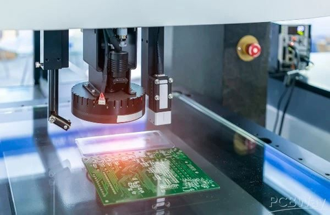
Wafer Inspection and Metrology Equipment
Inspection and measurement systems identify defects and evaluate dimensions, film thickness, surface quality, and pattern accuracy.
Dicing and Packaging Equipment
Dicing machines separate individual chips from wafers, while packaging equipment assembles and protects semiconductor dies.
Benefits of Advanced Microchip Manufacturing
Advanced semiconductor manufacturing provides several benefits to the electronics and technology industries.
1. Higher Processing Performance
Modern fabrication technologies allow manufacturers to develop powerful processors with advanced computing capabilities.
2. Improved Energy Efficiency
Optimized chip architectures and manufacturing processes can reduce power consumption while supporting demanding electronic applications.
3. Smaller Electronic Devices
Miniaturized semiconductor structures make it possible to manufacture compact electronic products with advanced functionality.
4. Greater Functional Integration
Integrated circuits can combine multiple electronic functions within a single semiconductor device.
This reduces the need for separate components in many electronic systems.
5. Improved Reliability
Advanced manufacturing controls, inspection processes, and testing procedures help identify defects and support consistent product quality.
6. Support for Technological Innovation
Microchips enable developments in artificial intelligence, robotics, telecommunications, healthcare technology, automotive electronics, and industrial automation.
Industrial Applications of Microchip Manufacturing
Microchips are used in almost every major technology sector.
Consumer Electronics
Smartphones, laptops, televisions, cameras, gaming systems, and wearable devices depend on semiconductor chips for processing, storage, connectivity, and power management.
Automotive Industry
Modern vehicles use microchips for engine management, safety systems, infotainment, battery management, driver assistance, and electric powertrains.
Healthcare Industry
Medical equipment uses semiconductor technology in imaging systems, patient monitoring devices, diagnostic instruments, laboratory equipment, and wearable health devices.
Industrial Automation
Factories use microchips in programmable logic controllers, robotic systems, sensors, motor drives, machine vision equipment, and industrial communication networks.
Telecommunications
Communication infrastructure relies on semiconductor devices for signal processing, wireless connectivity, optical networks, and data transmission.
Artificial Intelligence and Data Centers
AI accelerators, graphics processors, memory chips, and networking components support demanding computing workloads in data centers and advanced computing facilities.
Aerospace and Defense
Specialized semiconductor devices support navigation, communication, control systems, monitoring equipment, and other electronic applications that require specific performance and reliability characteristics.
Challenges in Microchip Manufacturing
Despite technological advancements, semiconductor manufacturing involves significant operational and engineering challenges.
High Capital Investment
Building a semiconductor fabrication facility requires substantial investment in buildings, specialized machinery, cleanroom infrastructure, utilities, and manufacturing systems.
Strict Contamination Control
Tiny particles and chemical impurities can damage semiconductor structures. Maintaining cleanroom conditions is therefore essential.
Complex Manufacturing Processes
Modern chip fabrication involves hundreds or thousands of individual processing steps, depending on the device and manufacturing technology.
Each step requires precise control and careful process coordination.
High Energy and Water Consumption
Semiconductor fabrication requires substantial electricity and ultra-pure water for equipment operation, cooling, and wafer processing.
Efficient resource management is an important operational priority.
Equipment and Material Availability
Advanced semiconductor production depends on specialized equipment, high-purity materials, and complex international supply chains.
Disruptions can affect production schedules and manufacturing capacity.
Yield Management
Manufacturing yield refers to the proportion of functional chips produced from a wafer or production batch.
Defect reduction, process optimization, and advanced inspection are important for improving yield and controlling production costs.
Future Trends in Microchip Manufacturing
The semiconductor industry continues to evolve as demand increases for advanced computing, connectivity, and energy-efficient electronics.
Advanced Lithography
Advanced lithography technologies help manufacturers create increasingly sophisticated semiconductor structures and support the development of leading-edge chips.
3D Semiconductor Packaging
Three-dimensional packaging allows multiple semiconductor dies to be integrated into compact structures, improving system integration and supporting high-performance computing.
Artificial Intelligence in Manufacturing
AI-based systems can analyze production data, identify process variations, support predictive maintenance, and improve defect detection.
Advanced Semiconductor Materials
Materials such as silicon carbide (SiC) and gallium nitride (GaN) are becoming increasingly important in power electronics and high-frequency applications.
Chiplet Architecture
Chiplet-based designs combine smaller semiconductor dies within a single package. This approach can provide greater design flexibility and support advanced computing systems.
Sustainable Semiconductor Production
Manufacturers are increasingly focusing on energy efficiency, water recycling, chemical management, and reducing the environmental impact of semiconductor production.
Conclusion
Microchip manufacturing is a highly advanced industrial process that supports modern electronics, computing, communication, transportation, and automation. It involves several precision operations, including wafer preparation, photolithography, etching, deposition, doping, testing, and packaging.
The industry depends on specialized machinery, high-purity materials, advanced engineering, and strict contamination control to produce reliable semiconductor devices.

Related Post...
Discover China’s Top Electronics Manufacturers Shaping Global Tech
Updated: November 02, 2026
Read More
Microchip Manufacturing: Process, Technology, Equipment, and Applications
Updated: November 02, 2026
Read More
Inspection Machines: Types, Applications, Benefits, and Industrial Uses
Updated: November 02, 2026
Read More