High-Volume Industrial PCB Assembly Plants: Discover Automated Assembly Processes
High-volume industrial PCB assembly plants are built around precision, repeatability, and tightly controlled production flows.
Printed circuit boards must be populated with large numbers of electronic components while maintaining consistent placement, solder quality, electrical performance, and traceability.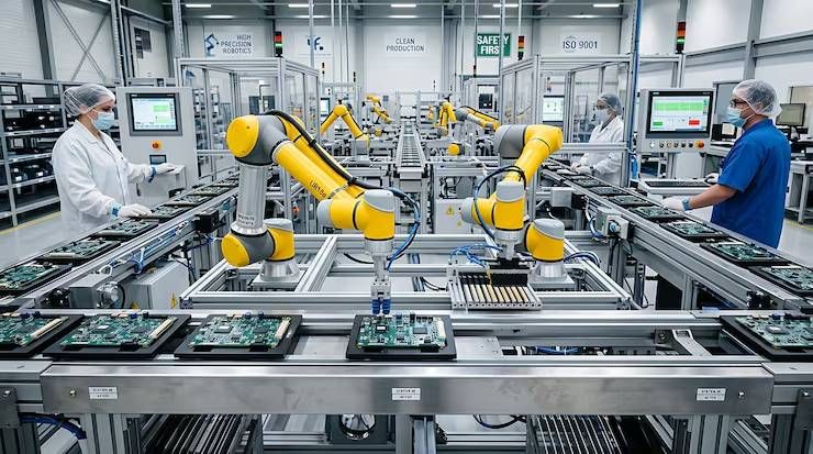
As industrial equipment becomes more connected and electronically controlled, PCB assemblies have become central to automation systems, power equipment, control panels, instrumentation, robotics, and industrial communication systems. High-volume production therefore requires more than fast machines; it requires an integrated manufacturing process.
Understanding automated PCB assembly means looking at the complete production sequence, from bare board preparation and component placement to soldering, inspection, testing, and production data management. Each stage contributes to the reliability of the finished assembly.
How High-Volume PCB Assembly Is Organized
Industrial PCB production typically follows a structured sequence in which each operation prepares the board for the next stage. Automation allows manufacturers to repeat these operations with consistent machine settings and controlled process parameters.
The production environment may include surface-mount technology (SMT) lines, through-hole assembly equipment, automated optical inspection systems, soldering systems, testing stations, and material-handling equipment.
The exact configuration depends on the board design and production requirements. A board containing thousands of small surface-mount components will require a different production strategy from one containing large connectors, transformers, or other through-hole components.
The objective is to create a continuous manufacturing flow where materials, machines, inspection points, and operators work together without unnecessary interruptions.
Preparing the PCB Before Component Placement
Production begins with the bare printed circuit board and the materials required for assembly. Before the board enters automated equipment, manufacturers verify its design data, board condition, component information, and production requirements.
Solder paste printing is often one of the first major automated operations in an SMT line. A stencil is positioned over the PCB, and solder paste is deposited onto designated pad locations.
The amount and position of solder paste matter greatly. Too little material can produce weak or incomplete solder joints, while excessive paste can contribute to bridging between closely spaced pads.
Automated solder paste inspection can evaluate deposited paste for characteristics such as volume, height, area, and alignment. Detecting problems at this stage helps prevent defects from progressing further through the production line.
Automated Component Placement
After solder paste application, the PCB moves to pick-and-place equipment. These machines retrieve electronic components from feeders and position them on the appropriate locations of the board.
Modern placement systems can handle extremely small components at high speed while maintaining precise positional accuracy. Machine vision helps identify component orientation and alignment before placement.
The feeder system is also critical because high-volume lines may require hundreds of component positions. Proper material loading and verification help prevent incorrect components from entering the assembly process.
Production software can connect placement programs with the board's bill of materials and design information. This coordination reduces manual intervention and supports repeatable manufacturing across large production runs.
Reflow Soldering Creates the Electrical and Mechanical Connection
Once surface-mount components are placed, the board typically passes through a reflow oven. Controlled heating melts the solder paste and allows it to form permanent connections between components and PCB pads.
The reflow process is divided into temperature zones. The board gradually heats, reaches the required soldering conditions, and then cools under controlled conditions.
Temperature profiling is essential because different components and board constructions can respond differently to heat. A poorly controlled profile can contribute to issues such as insufficient soldering, component damage, solder voids, or excessive thermal stress.
For high-volume production, consistent thermal profiles help maintain similar soldering conditions from one board to the next. Process monitoring can also identify deviations before they become widespread production problems.
Where Through-Hole Assembly Fits
Not every industrial PCB can be assembled entirely with surface-mount technology. Larger components, connectors, terminals, transformers, and mechanically demanding parts may still use through-hole technology.
In through-hole assembly, component leads pass through holes in the PCB and are soldered to conductive areas on the opposite side. Depending on the production requirements, components may be inserted manually, semi-automatically, or with automated insertion equipment.
Wave soldering is commonly associated with larger-scale through-hole production. The assembled board passes over a controlled wave of molten solder, allowing exposed component leads to form solder connections.
Some boards use a combination of SMT and through-hole technologies. These mixed-technology assemblies require careful sequencing because components placed during one stage must remain secure and protected during subsequent soldering operations.
Automated Inspection Protects Production Quality
Inspection is integrated throughout a modern PCB assembly line rather than being treated as a single final checkpoint.
Automated optical inspection (AOI) uses cameras and image-processing systems to examine populated boards. Depending on the system and programming, AOI can identify problems involving component presence, orientation, placement, solder joints, and visible defects.
Three-dimensional inspection can provide additional information about component height and solder characteristics. This can be particularly useful when conventional two-dimensional imaging cannot fully characterize a joint.
X-ray inspection may be used for assemblies where important solder connections are hidden beneath components. It can help identify issues such as voids, insufficient solder, misplaced components, and other internal defects.
These inspection technologies are valuable in high-volume environments because they can examine large numbers of assemblies consistently while generating production records for further analysis.
Electrical Testing Verifies Functional Performance
Visual inspection alone cannot confirm that an electronic assembly performs its intended function. High-volume industrial PCB plants therefore use electrical and functional testing appropriate to the product.
In-circuit testing can evaluate specific electrical characteristics and identify certain assembly faults. Functional testing goes further by operating the board under defined conditions to verify that its circuits perform as intended.
Testing may involve controlled signals, power inputs, communication interfaces, sensors, outputs, or other application-specific functions.
The test strategy depends heavily on the board's design. A controller used in industrial automation may require very different functional tests from a power-management board or communication module.
Production Traceability Matters at Industrial Scale
High-volume assembly requires strong traceability because a manufacturing defect can affect a large number of boards if it remains undetected.
Manufacturers may track information such as:
- PCB identification
- Component batches
- Production date and time
- Machine and line information
- Inspection results
- Soldering process data
- Test results
- Rework records
This information creates a production history for individual assemblies or defined production batches.
Traceability is particularly valuable when investigating recurring defects. Engineers can compare production data and identify whether a problem is associated with a particular component lot, machine setting, process stage, or manufacturing period.
How Automation Improves Production Consistency
Automation does more than increase production speed. Its larger value comes from controlling repetitive processes with consistent parameters.
A modern assembly line can coordinate material movement, machine programs, inspection results, and production records. Manufacturing execution systems can provide additional visibility by connecting production activities with planning and quality information.
Automation also reduces unnecessary manual handling. This can lower the risk of component damage, incorrect placement, contamination, and operator-to-operator variation.
However, automation does not eliminate the need for skilled personnel. Engineers, technicians, and quality specialists remain responsible for programming equipment, analyzing defects, maintaining machines, optimizing processes, and responding to production abnormalities.
Managing Defects in High-Volume Production
Even highly automated PCB assembly can experience defects. The key difference is how quickly a manufacturing operation can detect and control them.
Common assembly problems include solder bridges, insufficient solder, component misalignment, missing components, incorrect orientation, tombstoning, and contamination.
When an inspection system identifies an abnormality, manufacturers can investigate the process rather than simply removing the defective board. Root-cause analysis may involve reviewing stencil conditions, feeder performance, placement accuracy, reflow profiles, component batches, or PCB characteristics.
Statistical process control can also help identify gradual changes before they produce large numbers of defective assemblies. This approach shifts quality management from simple detection toward process control.
Designing PCB Assemblies for Automated Production
The manufacturing process begins with the board design itself. PCB designers can make production more reliable by considering how components will be placed, soldered, inspected, and tested.
Design for manufacturability, commonly called DFM, helps identify potential production problems before the board reaches the factory floor. Component spacing, pad geometry, thermal considerations, test access, board orientation, and assembly sequence can all affect manufacturability.
Design for testability is equally relevant. Test points and accessible electrical nodes can make automated testing easier and improve fault diagnosis.
A well-designed board therefore supports not only electrical performance but also efficient assembly, inspection, testing, and maintenance.
Frequently Asked Questions
What is automated PCB assembly?
Automated PCB assembly uses specialized machinery and software to place, solder, inspect, and test electronic components on printed circuit boards. It is commonly used when consistent and repeatable production is required.
What is the difference between SMT and through-hole assembly?
SMT components are mounted directly onto PCB surface pads, while through-hole components use leads that pass through holes in the board. Industrial assemblies may use either technology or a combination of both.
Why is solder paste inspection important?
Solder paste inspection checks whether the correct amount of solder paste has been deposited in the correct locations. Problems detected early can be corrected before components are permanently soldered.
How are assembled PCBs tested?
Depending on the product, manufacturers may use automated optical inspection, X-ray inspection, in-circuit testing, functional testing, or a combination of these methods.
Why is traceability important in high-volume PCB production?
Traceability allows manufacturers to connect individual assemblies or batches with production, inspection, component, and testing information. This makes defect investigation and quality control more effective.
Conclusion
High-volume industrial PCB assembly depends on a coordinated sequence of material preparation, solder paste printing, automated placement, soldering, inspection, testing, and traceability. Each stage contributes to the consistency and reliability of the finished electronic assembly.
Automation provides the repeatability needed for large production volumes, but successful manufacturing still depends on engineering discipline, process control, equipment maintenance, and effective quality management. When PCB design and factory processes are developed together, manufacturers can create assembly operations that are efficient, traceable, and capable of maintaining consistent production quality.

Related Post...
Wire Mesh Conveyor Belt: Explore Designs for Industrial Material Handling
Updated: October 06, 2026
Read More
Specialized Laboratory Diagnostics Automation: Explore Modern Testing Workflows
Updated: October 01, 2026
Read More
Intermodal Freight Transportation Operations: Explore How Cargo Moves Across Modes
Updated: October 01, 2026
Read More